Design Phase
Design Phase
The design phase consists of the following steps:
Concept - This is the initial idea.
Research - This is the detailed research regarding the technology required, possible vendors, material and design costs, and a feasibility study.
Circuit Design - This is the schematic diagrams, printed circuit layouts, and product enclosure designs.
The schematic in the figure is known as a circuit diagram. It is a graphical representation of an electrical circuit. A circuit diagram shows the components and interconnections of the circuit using standardized symbolic representations. The presentation of the connections between the circuit components in the diagram does not necessarily correspond to their physical arrangement in the finished device. A pictorial circuit diagram uses simple images of the components and their physical connection.
Prototype Phase
The prototype phase consists of the following steps:
Hardware, Mechanical, and Software Development - Software is a significant part of the project. Like the hardware, it should start with the high-level design.
PCB layout - The printed circuit board (PCB) design is a major element in electronics hardware development. Signal integrity tests should be carried out as part of this activity. Normally PCB CAD software packages are used to create the designs.
Build prototypes - Build the prototype of the finished product including graphics and packaging.
Product Testing - Thorough product testing and Test Readiness Review (TRR) is required before moving on to the next phase.
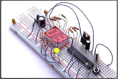
Solderless Breadboard
A solderless breadboard is a tool commonly used in electronic prototyping. The solderless breadboard provides the ability to create temporary circuits by plugging components into holes arranged in rows and columns across the surface, as shown in Figure 1. Circuits can be quickly created and taken apart by plugging and unplugging components like resistors and LEDs into the various rows and columns. The holes in the breadboard are contact holes with copper rails underneath the plastic surface, shown in Figure 2. Because the breadboard is solderless, it is a reusable prototyping tool making it easy to create temporary prototypes and experiment with circuit design.
Example:
Lab - The instructor must use the appropriate elements at his disposal to make the different demonstrations.
Production Phase
The production phase consists of the following steps:
Production Readiness Review - This step should be undertaken before the product is launched into full production.
Production - At this point all of the equipment should have been tested.
On-going Maintenance - Even when a product has entered production, on-going design maintenance is needed. Component obsolescence, design problems previously unnoticed, minor enhancements and other issues will all need to be addressed.
Printed Circuit Board (PCB)
A printed circuit board (PCB), shown in the figure, mechanically supports and electrically connects electronic components. A PCB uses conductive tracks, pads and other features etched from copper sheets and laminated onto a non-conductive substrate. Components, such as capacitors, resistors or active devices, are generally soldered on the PCB.
PCBs can be single-sided (one copper layer), double-sided (two copper layers) or multi-layer (outer and inner layers). Conductors on different layers are connected using small opening in the board called vias. Multi-layer PCBs allow for many more components than single- or double-sided PCBs of the same size.
PCBs are used in all but the simplest electronic products. Alternatives to PCBs include wire wrap and point-to-point construction. PCBs require the additional design effort to lay out the circuit, but manufacturing and assembly can be automated. Manufacturing circuits with PCBs is cheaper and faster than with other wiring methods, as components are mounted and wired with one single part. Furthermore, operator wiring errors are eliminated.