Physical inspection of the device for reverse engineering of IoT and Toys
Objectives: The goal in the context of the project is to accumulate knowledge about physical inspection of the device. What basic methods for reverse engineering of IoT and Toys?
We will present a general methodology for “blackbox” reverse engineering of IoT devices. The techniques presented address many use cases and can be used for gaining internal access to new devices. Most of the used techniques are generally well known, and they can be applied to many different IoT devices.

Block diagram, describing the structure of a typical IoT device:

The building blocks of black-box reverse engineering
Embedded Device Software Architectures
Software architecture (which may include an OS) determines many of the properties and limitations of a device. We distinguish between three main types of software architectures that are present in embedded devices.
Full stack OS based devices - devices that contain a modern operating system, such as Linux, that separates execution into kernel mode and user mode. While traditionally this architecture was preferred only when versatility and high performance was needed, more and more low-cost devices are now based on Linux due to falling component costs and the ease of developing for this operating system. In particular, many of the cameras we surveyed had a full stack Linux implementation.
Partial stack OS based devices - devices with a specifically designed RTOS (real-time operating system) such as VxWorks or vendor-provided OS implementation. These devices are generally specially crafted for their task [20], and tend to omit some of the features of full stack OSs. Some lower-end or single tasked IoT devices use this architecture, with the RTOS handling Wi-Fi and Web protocols, and additional vendor code responsible for gathering sensor data.
Devices with no operating system - embedded devices which directly execute compiled instructions, without any OS support for functionalities such as threading or interrupts. Devices with no OS can offer better raw performance and higher run-time predictability than other architecture, but tend to be more difficult to development, and therefore have a longer time-to-market (TTM).
Thus far, all of the IoT hacks have targeted full stack OS devices, as these are more generic and make use of various drivers and open source components that may have known vulnerabilities. For this reason, full stack OS devices have significant potential for security vulnerabilities as well.
Usually black-box reverse engineering process follows:
- Physical inspection of the device;
- Extraction of the device firmware image and file system;
- Bypass boot-time security and recover the firmware image;
- Recover the data with out-of-band means;
- Analysis the firmware image and recovery of the new one inside it.
A. Physical inspection of the device
Electronic devices are usually held together by screws or plastic clips. Most of the devices can be opened without damaging the exterior of the device or the internal components. Some device manufacturers also use glue during assembly, thus making opening the device more difficult.
1) Locating and identifying memory components: Smart devices that run the Linux operating system require sufficient non-volatile memory to store the kernel and other mandatory file system components. A cheap and efficient way for engineering such devices is to place the memory module outside of the main processor package. Devices engineered in such configurations usually employ a processor that is capable of loading and running instructions directly from the SPI (serial parallel interface) Flash memory or EEPROM devices.
Understanding the memory technology is crucial for performing firmware extraction when there is no possibility of running commands on the tested device.
A memory module that uses technology consistent with the required capacity is often found in devices. Common examples are: 25XX \ 26XX series eight-pin SPI Flash memory with up to 32MB of storage space; larger SPI Flash devices with sixteen or thirty-two pins; NAND Flash devices that come in various capacities and shapes and are usually coupled with a 24XX EEPROM module for holding initial configuration; eMMC (embedded multimedia controller) modules or cards usually containing more than a gigabyte of data.
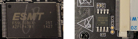
Examples of memory modules
Identification of the memory module can be performed by searching the engraved device codes on the IC (integrated circuit) package. In most cases the modules used are commonly known and available off-the-shelf with publicly available datasheets.
2) Locating UART terminals: UART (universal asynchronous receiver/transmitter) ports are embedded universal communication channels with many purposes. Within smart devices, UART ports are commonly used for development and maintenance via a Linux console that the port is bound to. UART ports communication is based on a standard protocol at a predetermined baud rate. Typical baud rates for UART communication with embedded devices are 9600, 57000, and 115200 bits-per-second.
In many cases, UART terminals are embedded into the PCB (printed circuit board) in the prototyping stages of a product’s life and are kept in the design during production either to reduce costs of redesign or maintain access for future maintenance. In certain cases, UART terminals are placed in visible and accessible locations, occasionally marked with their purpose. In other cases, the terminals are hidden (intentionally or unintentionally) between other test points exposed on the boards for post-production testing. Connecting to UART terminals allows easy access for communication with the OS and may also form a beachhead for the benefit of reverse engineering.
Basic UART communication requires only three electrical lines: TX (transmit), RX (receive) and GND (ground). A typical UART terminal has two to four exposed copper pads aligned in a row; when there are two pads, the TX pad is pulled electrically towards +1.8v, +3.3v or +5v and the RX pad might not be pulled to either directions; when there are three pads, the additional pad is usually the GND pad which should have continuity to the ground plane of the PCB; when there are four pads, the last pad is generally a VCC (positive voltage supply) which shows up as +1.8v, +3.3v or +5v when powered on.
By using the typical properties and appearances of UART terminals it is possible to locate suspected terminals using a multimeter and verify them by attaching a digital analyzer capable of analyzing UART communication.
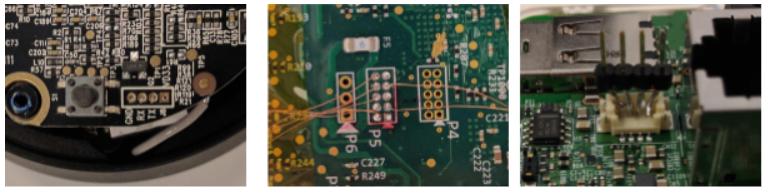
Figures showing various placements of UART terminals
3) UART discovery assistant module: In order to assist in the detection of UART terminals on PCBs that contain a large amount of test points, usually some logical analyzer device are used. The simplest devices is composed of an programmable micro-controller along with auxiliary electronics with custom code that switches between popular UART baud rates, and it beeps when encountering a specified number of English printable ASCII characters (characters with an ASCII denotation larger than 0x20 and smaller than 0x7F).
Retrieval of data from within the device is a key component of reverse engineering.
Additional Reading Here